
Introduction / Industry Overview
Medical electronics occupies the apex of PCB design rigor—a domain where a solder joint failure is not a warranty claim but a patient safety event. The global medical electronics market was valued at approximately USD 190 billion in 2025, projected to exceed USD 300 billion by 2030 (Grand View Research, 2025), driven by the proliferation of wearable health monitors, minimally invasive surgical systems, AI-powered diagnostic imaging, and the ongoing digitization of hospital infrastructure.
What distinguishes medical electronics from every other PCB design discipline is the regulatory weight behind every design decision. IEC 60601-1 (medical electrical equipment safety), ISO 13485 (quality management systems), ISO 10993 (biological evaluation), and FDA 21 CFR Part 820 (quality system regulation) establish a compliance framework that permeates material selection, layout architecture, manufacturing process control, testing protocols, and documentation requirements. A medical PCB is not merely designed—it is validated, verified, and documented to a standard that makes the resulting technical file a regulatory artifact as much as an engineering deliverable.
This article examines the core technologies, application cases, and future trajectory of medical electronics PCB design, with emphasis on the IEC 60601 safety framework, biocompatibility requirements for implantable and skin-contact devices, and the manufacturing discipline demanded by ISO 13485.
Core Technology Analysis
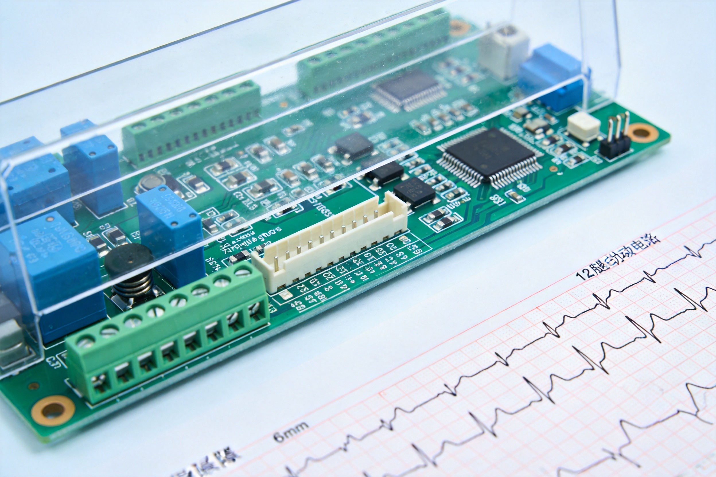
IEC 60601 Safety Framework: Electrical Isolation and Creepage/Clearance
IEC 60601-1 is the foundational safety standard for medical electrical equipment, now in its 3.2 edition (2020). Its requirements directly shape PCB layout through two primary mechanisms: electrical isolation and creepage/clearance distances.
Electrical Isolation: Medical devices that make patient contact (e.g., ECG electrodes, surgical instruments, patient monitors) must maintain at least two levels of protection (Means of Protection, MOP) between the patient connection and hazardous voltage sources. On the PCB, this translates to:
- Reinforced insulation between primary (mains-connected) and secondary (patient-connected) circuits, typically achieved through isolated DC-DC converters providing 1500 Vrms (for 230 VAC mains) or 4000 V (for defibrillator-proof equipment) dielectric withstand
- Galvanic isolation of patient-connected analog front ends (ECG, EEG, SpO2) from digital processing sections, using digital isolators (e.g., ADI iCoupler series, 5000 Vrms isolation) or optocouplers
- Separate ground domains: The patient ground (reference electrode) must never share a return path with equipment ground or chassis ground. The PCB must maintain physically separated ground planes connected only through the isolation barrier
Creepage and Clearance: IEC 60601-1 tables specify minimum distances based on working voltage, pollution degree, and material group. For a typical 240 VAC medical device (Pollution Degree 2, Material Group IIIa):
| Voltage | Basic Insulation Clearance | Reinforced Insulation Clearance | Creepage (Basic) | Creepage (Reinforced) |
|---|---|---|---|---|
| 240 VAC | 1.6 mm | 3.2 mm | 2.5 mm | 5.0 mm |
| 500 VAC | 3.0 mm | 6.0 mm | 5.0 mm | 10.0 mm |
These distances are enforced through isolation slots—routed gaps in the PCB that physically separate primary and secondary circuits. Slots must be at least 1 mm wide (wider for higher voltages) and must not have any copper or components spanning the gap. In multilayer boards, the isolation must extend through all layers, including internal ground planes.
Leakage Current Limits: IEC 60601-1 restricts patient leakage current to 10 μA (normal condition) for Type CF (cardiac floating) applied parts—the most stringent classification. This limit directly constrains PCB layout: parasitic capacitance between isolated domains (which increases with overlapping copper areas and decreases with distance) must be kept below approximately 100 pF to meet the 10 μA limit at 50/60 Hz. This means primary and secondary ground planes must not overlap across the isolation barrier.
Biocompatibility: ISO 10993 for Implantable and Skin-Contact Devices
For PCBs that contact human tissue—whether through implantation (pacemakers, neurostimulators) or skin contact (wearable monitors, TENS units)—ISO 10993 biological evaluation is mandatory. The standard requires a risk-based assessment of all materials in the device’s construction, including PCB substrates, solder alloys, surface finishes, conformal coatings, and encapsulation compounds.
Key ISO 10993 Tests for PCB Materials:
| Test | Standard | Acceptance Criteria |
|---|---|---|
| Cytotoxicity | ISO 10993-5 | >70% cell viability in extract test |
| Sensitization | ISO 10993-10 | No allergic response in guinea pig maximization test |
| Irritation | ISO 10993-10 | No significant erythema/edema in rabbit skin test |
| Systemic toxicity | ISO 10993-11 | No adverse systemic effects in mouse injection test |
| Genotoxicity | ISO 10993-3 | Negative in bacterial reverse mutation (Ames) test |
Substrate Material Selection:
- Standard FR-4: Adequate for non-implantable, non-contact devices (e.g., hospital equipment with hermetically sealed enclosures). Must be fully encapsulated under conformal coating or potting compound with no direct tissue exposure.
- Polyimide (PI): Preferred for implantable flex circuits. USP Class VI certified grades are available with demonstrated biocompatibility per ISO 10993-5. CTE of ~20 ppm/°C closely matches copper (17 ppm/°C), reducing thermal cycling stress.
- Liquid Crystal Polymer (LCP): Emerging substrate for implantable applications with superior moisture barrier properties (water absorption <0.04% vs. 1–3% for polyimide) and stable dielectric properties. LCP flex circuits have passed 21-day implantation simulation testing.
- PTFE composites: Used in high-frequency medical imaging (MRI coils, ultrasound transducers) where low dielectric loss is critical.
Surface Finish Selection: ENIG (Electroless Nickel Immersion Gold) is the industry standard for medical PCBs, providing excellent solderability, wire-bondability, and shelf life. For implants, the nickel layer must be fully encapsulated—exposed nickel can cause allergic reactions in sensitive patients. ENEPIG (Electroless Nickel Electroless Palladium Immersion Gold) adds a palladium barrier that prevents nickel migration and provides additional corrosion resistance.
Encapsulation: Implantable PCBs require hermetic sealing—typically a titanium can with laser-welded feedthroughs for electrical connections, or medical-grade silicone rubber (ISO 10993-compliant) encapsulation for flexible implants. Parylene (poly-para-xylylene) conformal coating at 5–25 μm thickness is widely used for both implantable and skin-contact devices, providing excellent moisture barrier properties, biocompatibility, and dielectric strength (>7 kV/mil).
ISO 13485 Manufacturing Discipline: Traceability and Process Control
ISO 13485 certification is non-negotiable for any PCB manufacturer serving the medical device industry. It mandates:
- Complete traceability: Every raw material lot, every process parameter, every test result, and every operator involved in producing a specific PCB must be documented and retrievable for the device’s lifetime (minimum 7 years, often 15+ years). Barcode- or RFID-based tracking systems link each board to its complete manufacturing history.
- Process validation: Critical manufacturing processes (lamination temperature/time/pressure, etching uniformity, plating thickness, reflow profile) must be validated with three consecutive production runs of 100+ units, each achieving ≥99.9% defect-free yield.
- Change control: Any change to materials, processes, or suppliers requires formal risk assessment, verification testing, and regulatory notification before implementation. This includes changes at the PCB manufacturer’s subcontractors.
- Corrective and Preventive Action (CAPA): Any defect detected during manufacturing, testing, or field use triggers a root-cause analysis, corrective action, and preventive measures to avoid recurrence.
Testing Requirements: Medical PCBs undergo 100% electrical testing (flying probe or bed-of-nails), 100% automated optical inspection (AOI), X-ray inspection for BGA/QFN solder joints, and environmental stress screening (thermal cycling, burn-in) for safety-critical applications. Ion contamination testing per IPC-5704 must demonstrate cleanliness levels below 1.0 μg NaCl equivalent/cm²—significantly stricter than the 2.0 μg/cm² standard for non-medical applications.
Low-Noise Design for Diagnostic Signal Acquisition
Medical diagnostic signals are among the weakest in electronics: ECG signals range from 0.5–5 mV, EEG from 10–100 μV, and neural recordings from single neurons as low as 10–100 μV. The PCB must preserve these microvolt-level signals in the presence of 50/60 Hz power-line interference, RF interference from surgical equipment and mobile devices, and thermal noise from the analog front end.
Key PCB Design Techniques:
- Driven-right-leg (DRL) circuit: An active feedback loop that drives the patient’s reference electrode to cancel common-mode interference, achieving >80 dB common-mode rejection at 50/60 Hz.
- Guard ring implementation: A grounded copper ring surrounding high-impedance input traces (ECG, EEG electrodes) that intercepts leakage currents before they reach the sensitive input nodes.
- Chopper-stabilized amplifiers: Auto-zeroing amplifiers (e.g., ADI AD8422, 1.5 μV offset, 0.01 μV/°C drift) eliminate 1/f noise and offset drift that would otherwise overwhelm microvolt-level signals.
- Power supply isolation: The analog front end is powered through an isolated DC-DC converter with post-regulation by ultra-low-noise LDOs (LT3042, 0.8 μV RMS output noise), ensuring that switching power supply ripple does not couple into the measurement path.
Typical Application Cases
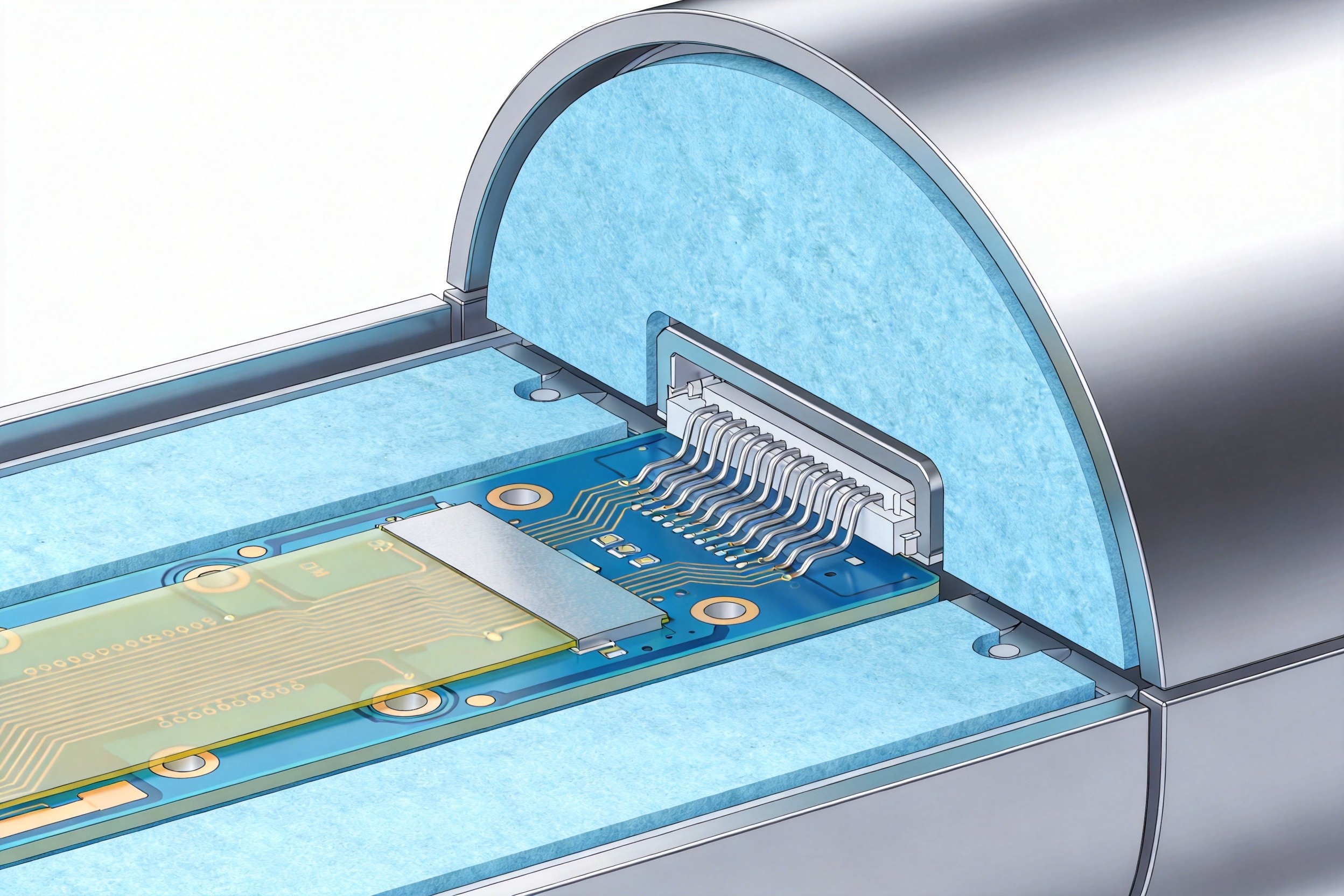
Case 1: 12-Lead Diagnostic ECG — Microvolt Signal Integrity
A 12-lead diagnostic ECG must detect 5 μV signals (P-wave amplitude in some pathologies) with baseline drift below 10 μV/minute, in the presence of 50/60 Hz common-mode interference up to 1 V.
PCB Design Approach: 8-layer board with separated analog front-end (AFE) and digital processing sections. Each of the 12 channels uses a dedicated AD8422 instrumentation amplifier (1.5 nV/√Hz input noise, 80 dB CMRR at 1 kHz) followed by a 24-bit delta-sigma ADC (ADS124S08, 19 nV input-referred noise at PGA = 128). The DRL circuit actively drives the patient’s right leg to cancel common-mode interference, achieving >100 dB effective CMRR at 50/60 Hz. Guard rings surround all electrode input traces on every layer. The AFE section is powered through an isolated DC-DC converter (5000 Vrms isolation, IEC 60601-1 compliant) with ultra-low-noise LDO regulation. The isolation barrier is implemented as a 6 mm slot across all PCB layers, with digital isolators (ADI ADuM1401) bridging the gap for SPI communication.
Result: Input-referred noise of 3 μV peak-to-peak (0.05–150 Hz bandwidth), CMRR of 102 dB at 50 Hz, patient leakage current of 4.2 μA (within the 10 μA IEC 60601-1 Type CF limit), and IEC 60601-1-2 EMC compliance (immunity to 10 V/m RF fields per IEC 61000-4-3).
Case 2: Implantable Neurostimulator — Biocompatibility and Ultra-Low Power
A spinal cord stimulator for chronic pain management must operate for 7+ years on an internal rechargeable battery, deliver programmable stimulation pulses (0.1–10 mA, 20–1000 μs pulse width), and maintain hermetic sealing within a titanium enclosure.
PCB Design Approach: 4-layer polyimide flexible PCB (USP Class VI certified, 0.1 mm thickness) folded into a cylindrical titanium can (6 mm diameter × 50 mm length). The stimulation ASIC is wire-bonded to the PCB with gold wires (25 μm diameter). Output coupling capacitors (medical-grade C0G MLCCs, 1 μF, rated to 100 V) provide DC-blocking to prevent tissue damage from DC current. The PCB surface is coated with 10 μm parylene-C for additional moisture protection. All solder is SAC305+Ni (medical-grade, ISO 10993-5 compliant). Battery management circuitry includes over-voltage, under-voltage, and over-current protection with redundant safety mechanisms. Total quiescent current: 8 μA (extending battery life to 9+ years between recharge cycles at typical usage).
Result: Zero cytotoxicity per ISO 10993-5, hermeticity verified by helium leak testing at <1×10⁻⁹ atm·cm³/s, stimulation output accuracy of ±3% over the full −10°C to +50°C operating range, and MRI conditional labeling approved for 1.5T and 3T scanners.
Case 3: Portable Ultrasound Probe — High-Frequency Signal Integrity
A handheld ultrasound probe with a 128-element phased array (center frequency 7.5 MHz, bandwidth 5–10 MHz) must maintain signal integrity across the high-density interconnect between the piezoelectric elements and the beamforming ASIC.
PCB Design Approach: 10-layer HDI rigid-flex PCB. The rigid section contains the beamforming ASIC (0.4 mm pitch BGA) and high-voltage pulsers (±100 V, 0.1–1 A peak), while the flexible section connects to the transducer array with 128 differential channel pairs (100Ω ±3% controlled impedance). The high-voltage pulser section uses 3 oz copper on outer layers with thermal via arrays, isolated from the low-noise receive section by ground-plane splits and a 0.5 mm air gap. Substrate materials: Rogers RO4350B for RF/microwave signal layers, high-Tg FR-4 for digital/power layers. Conformal coating with medical-grade silicone for IPX7 waterproofing.
Result: Channel-to-channel crosstalk below −70 dB at 7.5 MHz, insertion loss of 0.8 dB per channel across the flex interconnect, and IEC 60601-1 compliance with patient leakage current below 50 μA (Type BF applied part).
Future Development Trends
Miniaturization and Implantable Bioelectronics
The convergence of flexible electronics, biocompatible materials, and ultra-low-power ASIC design is driving implantable devices toward sub-centimeter form factors. Neural dust—millimeter-scale wireless sensors powered by ultrasonic energy—represents the extreme miniaturization frontier, requiring PCBs (or their functional equivalents) fabricated on biocompatible thin films at feature sizes below 10 μm. Polyimide and Parylene-C multilayer constructions currently lead the field, but dissolvable electronics (silk fibroin substrates that resorb after a programmed lifetime) are entering clinical trials for post-surgical monitoring. Timeframe: Sub-centimeter implantable bioelectronics are in clinical trials (2025–2027); commercial deployment in select applications by 2028–2029.
AI-Enabled Diagnostics and Edge Computing in Medical Devices
The integration of neural network inference on medical device PCBs—from real-time arrhythmia detection in wearable ECG monitors to AI-assisted image analysis in portable ultrasound—is driving medical electronics toward heterogeneous computing architectures. Edge AI inference requires NPUs or GPU-class accelerators, LPDDR memory interfaces, and high-speed data paths, all while maintaining the electrical isolation, low leakage current, and EMC compliance mandated by IEC 60601. This creates a unique mixed-signal design challenge: ensuring that high-power AI computation bursts do not couple noise into sensitive diagnostic signal paths. Timeframe: AI-enabled diagnostic devices are already FDA-cleared (ECG, retinal imaging); next-generation AI+diagnostic integrated PCBs will emerge in 2027–2028.
Wireless Medical Telemetry and Remote Patient Monitoring
The expansion of remote patient monitoring (RPM) is driving medical PCBs to integrate wireless connectivity (BLE 5.x, Wi-Fi 6, cellular NB-IoT) alongside diagnostic signal acquisition. The PCB must accommodate both the RF front end (with its antenna and matching network requirements) and the isolated patient-connected analog circuits on the same board. Coexistence management—ensuring that wireless transmissions do not generate interference that degrades diagnostic accuracy—is a growing design challenge, particularly for wearable devices where the antenna and the ECG electrodes share the same physical space. Timeframe: Wireless RPM devices are in volume production; next-generation multi-sensor wireless diagnostic patches will be mainstream by 2027–2028.
Conclusion
Medical electronics PCB design is governed by a regulatory framework that makes no distinction between design elegance and patient safety—both are mandatory, and both must be documented, validated, and verified. The IEC 60601 safety requirements dictate isolation architecture, creepage distances, and leakage current limits that shape every layer of the PCB stackup. ISO 10993 biocompatibility requirements constrain material selection for every component of the PCB construction, from substrate to solder to coating. And ISO 13485 manufacturing discipline ensures that the validated design is reproduced with zero deviation across every production unit. As medical electronics evolve toward implantable bioelectronics, AI-enabled diagnostics, and wireless remote monitoring, the PCB designer’s challenge is expanding from “make it safe and accurate” to “make it safe, accurate, intelligent, connected, and implantable.” For electronics manufacturers entering the medical device supply chain, regulatory compliance is the entry ticket, and engineering excellence—demonstrated through robust isolation design, meticulous biocompatibility management, and verifiable process control—is what distinguishes trusted suppliers.
Need medical-grade PCB manufacturing with IEC 60601 and ISO 13485 compliance? Connect with our engineering team to discuss biocompatible material selection, isolation design support, and validated production capabilities.