


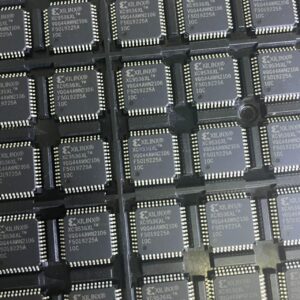
Product Overview
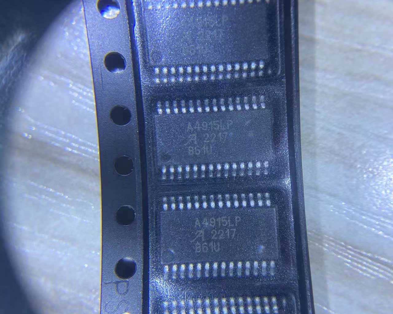
The A4915MLPTR-T is a three-phase MOSFET gate driver IC from Allegro MicroSystems, designed for pulse-width modulated (PWM) current control of 3-phase brushless DC (BLDC) motors. Capable of driving six N-channel power MOSFETs, the A4915 integrates block commutation logic, synchronous rectification control, and a speed input for analog duty cycle control, eliminating the need for a microcontroller PWM output in many simple speed control applications. The device operates from a 5V to 50V supply range with an internal charge pump that ensures full gate drive down to 7V supply (and limited drive down to 5V). Built-in features include Hall sensor inputs for direct commutation, adjustable dead time, cross-conduction protection, undervoltage lockout (UVLO), thermal shutdown, and a low-current sleep mode. Packaged in a 28-pin TSSOP with exposed thermal pad, the A4915MLPTR-T is ideal for battery-powered equipment, power tools, industrial motor control, robotics, and 2W chassis and safety applications where low voltage operation and high efficiency are critical.
Key Specifications
| Parameter | Value |
| Load Supply Voltage (VBB) | 5 V to 50 V operating range |
| Logic Supply Voltage (VDD) | 3.3 V to 5.5 V |
| Number of MOSFETs Driven | 6 (three-phase, all N-channel) |
| Gate Drive Type | N-Channel MOSFET, bootstrap high-side, charge pump low-side |
| Gate Drive Voltage | Full drive down to 7V VBB; limited drive down to 5V VBB |
| Commutation Method | Block (trapezoidal) commutation via Hall sensor inputs |
| PWM Control Method | Internal PWM via SPEED analog input or external PWM via ENABLE pin |
| PWM Frequency (Internal) | 30 kHz typical (center-aligned) |
| Control Inputs | ENABLE, DIR, BRAKEn, SPEED (analog), HA/HB/HC (Hall) |
| Synchronous Rectification | Internally controlled synchronous rectification |
| Dead Time | Adjustable via external resistor |
| Protection Features | UVLO, cross-over current protection, latched TSD with fault output |
| Sleep Mode Current | Low current sleep when ENABLE held low > tSLEEP |
| Charge Pump Stabilization Time | 3 ms max (coming out of sleep) |
| Operating Temperature Range | -40 degC to +150 degC junction |
| Package | 28-Pin TSSOP with Exposed Thermal Pad (LP package) |
| Packing | 4000 pieces per 13-in reel (tape and reel) |
| Lead Finish | 100% matte-tin (lead-free) |
Features
- 5V to 50V wide supply voltage range for diverse battery and bus voltages
- Drives six N-channel power MOSFETs for 3-phase BLDC motor control
- Integrated block commutation logic with Hall sensor inputs
- Internal charge pump ensures gate drive at low supply voltages
- Analog SPEED input provides 0-100% PWM duty cycle control
- Center-aligned PWM for reduced EMI and balanced power dissipation
- Internally controlled synchronous rectification for improved efficiency
- Adjustable dead time protection via external resistor
- Internal UVLO and crossover current protection
- Latched thermal shutdown (TSD) with fault output indication
- Brake mode (active-low) for FMEA compliance and emergency stop
- Low power sleep mode for battery-powered applications
- Direction control input for forward/reverse motor operation
- Enable input with external PWM control capability
- Exposed thermal pad package for enhanced heat dissipation
- Lead-free, 100% matte-tin plating
Applications
- Cordless power tools and garden equipment
- Industrial motor control and drives
- Robotics and robotic actuators
- E-bikes and light electric vehicles
- 2W chassis and safety systems
- Home appliances with BLDC motors
- Battery-powered pumps and fans
- Automotive auxiliary motor drives
- Consumer electronics with brushless motors