





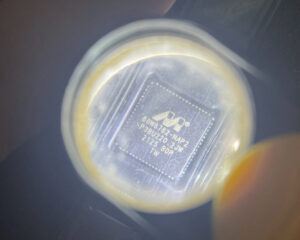
Product Overview
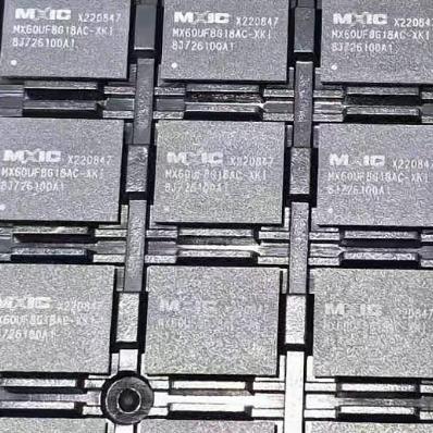
The MX60UF8G18AC-XKI is a 1.8V, 8Gb SLC (Single-Level Cell) NAND Flash Memory device from Macronix (MXIC), belonging to the MX60UF 1.8V family. It is stacked from two 4Gb die, each organized with two planes of 2048 blocks. The device features a (2048+64)-byte page size, (128K+4K)-byte block size, ONFI 1.0 compliant interface, and supports Cache Read/Cache Program and Two-Plane operations. The -XKI suffix denotes the 63-VFBGA (9mm × 11mm) package with industrial-grade temperature range (-40°C to +85°C). With a typical P/E endurance of 100K cycles (with 4-bit ECC per 528 bytes), it is well-suited for embedded system code and data storage in mobile, M2M, and low-voltage applications.
Key Specifications
| Manufacturer | Macronix (MXIC) |
| Density | 8Gb (1G × 8) |
| Cell Type | SLC (Single-Level Cell) |
| Voltage (VCC) | 1.7V – 1.95V |
| Bus Width | x8 |
| Interface | Parallel, ONFI 1.0 Compliant |
| Page Size | (2048 + 64) bytes |
| Block Size | (128K + 4K) bytes = 64 pages per block |
| Plane Size | 2 planes per die, 2048 blocks per plane |
| Die Stack | 2 × 4Gb die (Multi-die) |
| ECC Requirement | 4-bit ECC per (512+16) bytes |
| Random Read Access (tR) | 25 μs (typ.) |
| Sequential Read Speed | 25 ns per byte |
| Access Time | 22 ns |
| Page Program Time | 320 μs (typ.), 600 μs (max) |
| Block Erase Time | 1 ms (typ.), 3.5 ms (max) |
| Active Current | 30 mA (max) |
| Standby Current | 100 μA (max) |
| Endurance | 100,000 P/E cycles (typ.) |
| Data Retention | 10 years |
| Operating Temperature | -40°C to +85°C (Industrial) |
| Guaranteed Good Block | Block #0 at shipping |
| Secure OTP | Supported (30 pages) |
| Unique ID | ONFI standard |
| Electronic Signature | 5 cycles |
| Two-Plane Operations | Supported |
| Chip Enable Don’t Care | Supported |
| Package | 63-VFBGA, 9mm × 11mm, 0.8mm ball pitch |
| RoHS / Halogen-Free | Yes |
Features
- 8Gb SLC NAND Flash with high reliability (100K P/E cycles typical)
- 1.8V low-voltage operation (1.7V – 1.95V) for mobile and M2M applications
- Two 4Gb die stacked with interleaved die operation support
- ONFI 1.0 compliant parallel interface with command/address/data multiplexing
- Cache Read and Cache Program for improved throughput
- Two-Plane Program and Two-Plane Cache Program support
- Secure One-Time Programmable (OTP) area: 30 pages
- Unique ID Read (ONFI standard) and Electronic Signature (5 cycles)
- Hardware write protection via WP# pin
- Chip Enable Don’t Care for simplified system interface
- Low power: 30 mA active / 100 μA standby
- Industrial temperature range: -40°C to +85°C
Applications
- Mobile phones and 3G/4G/5G data cards requiring low-voltage NAND storage
- M2M (Machine-to-Machine) devices and IoT edge nodes
- Embedded system code and data storage in portable electronics
- Industrial control systems with 1.8V logic
- Boot code and configuration storage in low-power FPGA / SoC platforms