
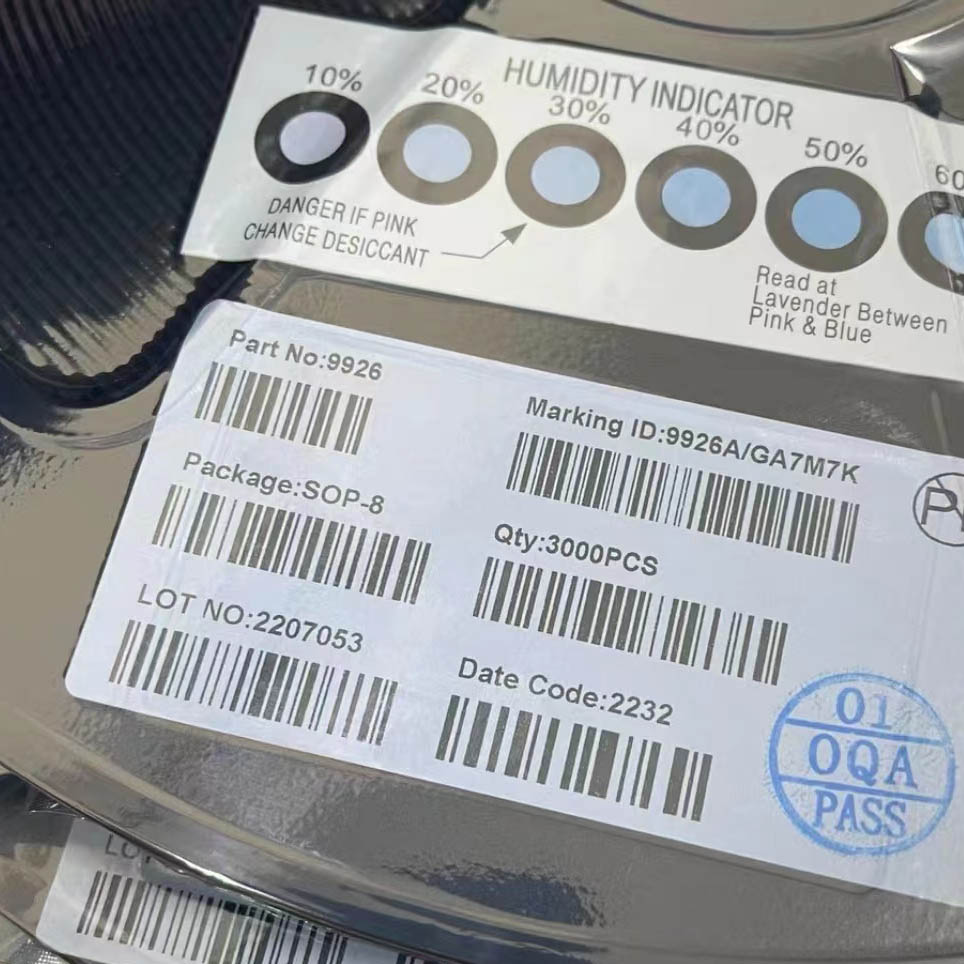



Product Overview
The AO9926A is a dual N-channel enhancement mode field effect transistor (MOSFET) manufactured using advanced trench technology, providing excellent RDS(ON) performance and low gate charge. The device contains two independent N-channel MOSFETs in a single SOIC-8 package, offering a space-saving solution for applications requiring two power switches. With a drain-source voltage rating of 20V and continuous drain current of 7A per channel, the AO9926A is well-suited for battery protection, load switching, and DC-DC converter applications. The device operates over a wide gate drive range from 1.8V to 8V, making it compatible with low-voltage logic-level control signals. The two MOSFETs can be used individually, in parallel for higher current capability, or configured to form a bidirectional blocking switch. The AO9926A is commonly used in lithium-ion battery protection circuits (BMS), portable electronics power management, and motor drive applications.
Key Specifications
| Parameter | Conditions | Min | Typ | Max | Unit |
| Configuration | Dual N-Channel | ||||
| Drain-Source Voltage (VDS) | 20 | V | |||
| Gate-Source Voltage (VGS) | ±8 | V | |||
| Continuous Drain Current (ID) | TA=25°C, VGS=4.5V | 7 | A | ||
| Pulsed Drain Current (IDM) | 30 | A | |||
| Power Dissipation (PD) | TA=25°C | 2 | W | ||
| RDS(ON) | VGS=4.5V, ID=7A, 25°C | 21.6 | 26 | mΩ | |
| RDS(ON) | VGS=4.5V, ID=7A, 125°C | 29.2 | 36 | mΩ | |
| RDS(ON) | VGS=2.5V, ID=5A | 26.4 | 33 | mΩ | |
| RDS(ON) | VGS=1.8V, ID=4A | 33.3 | 42 | mΩ | |
| Gate Threshold Voltage (VGS(th)) | VDS=VGS, ID=250μA | 0.3 | 0.5 | 0.8 | V |
| Zero-Gate Drain Current (IDSS) | VDS=16V, VGS=0V | 1 | μA | ||
| Gate-Body Leakage (IGSS) | VDS=0V, VGS=±8V | 100 | nA | ||
| Forward Transconductance (gFS) | VDS=5V, ID=5A | 22 | S | ||
| Input Capacitance (Ciss) | VGS=0V, VDS=10V | 1050 | pF | ||
| Output Capacitance (Coss) | VGS=0V, VDS=10V | 163 | pF | ||
| Reverse Transfer Cap (Crss) | VGS=0V, VDS=10V | 129 | pF | ||
| Total Gate Charge (Qg) | VGS=4.5V, VDS=10V, ID=7A | 15.2 | nC | ||
| Gate-Source Charge (Qgs) | 1 | nC | |||
| Gate-Drain Charge (Qgd) | 4 | nC | |||
| Turn-On Delay (td(on)) | 6.5 | 9 | ns | ||
| Turn-Off Delay (td(off)) | 56.5 | ns | |||
| Body Diode VSD | IS=1A | 0.76 | 1 | V | |
| Body Diode trr | 21 | ns | |||
| Body Diode Qrr | 7.1 | nC | |||
| Junction Temperature | 150 | °C | |||
| Package | SOIC-8 (SOP-8) | ||||
Features
- Dual N-channel enhancement mode MOSFET
- VDS: 20V, ID: 7A (per channel at 25°C)
- RDS(ON): 26mΩ max @ VGS=4.5V, ID=7A
- Low RDS(ON) at low gate voltages: 33mΩ @ 2.5V, 42mΩ @ 1.8V
- Advanced trench technology
- Low gate charge: 15.2nC typical
- Wide gate drive range: 1.8V to 8V
- Logic-level gate drive compatible
- High cell density for low RDS(ON)
- Two devices can be used in parallel or as bidirectional switch
- Fast switching speed
- Body diode with fast reverse recovery
- SOIC-8 package
- RoHS compliant and halogen-free
Applications
- Lithium-ion battery protection (BMS)
- Load switching in portable electronics
- DC-DC converters and power management
- Small motor drivers and motor control
- Notebook computers and tablets
- Smartphones and wearable devices
- Power management ICs (PMIC) companion
- Battery packs and chargers
- USB power switches
- Consumer electronics power rails