




Product Overview
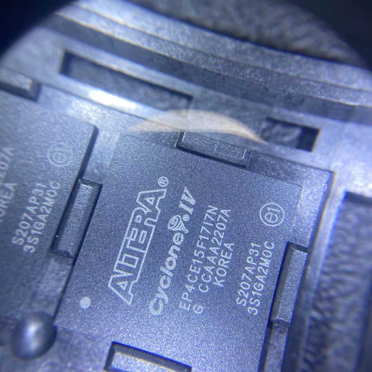
The EP4CE15F17I7N is a field-programmable gate array from Altera (now Intel) Cyclone® IV E family, offering a cost-optimized combination of logic, memory, and DSP resources with low power consumption. Housed in a 256-pin FineLine BGA package (17×17mm), this industrial-grade device features 15,408 logic elements (LEs), 56 M9K RAM blocks totaling 516 Kbits of embedded memory, 56 embedded 18×18 multipliers, 4 phase-locked loops (PLLs), 20 global clock networks, and up to 181 user I/O pins. Built on TSMC’s 60nm low-power process technology with a 1.0V/1.2V core, Cyclone IV E devices deliver the lowest static power in the Cyclone family. The -7 speed grade and industrial temperature range (-40°C to +100°C) make this device suitable for industrial control, automotive, communications, and consumer applications requiring reliable operation at low cost and low power.
Key Specifications
| Parameter | Value |
| Manufacturer | Altera (Intel® PSG) |
| Part Number | EP4CE15F17I7N |
| Product Family | Cyclone® IV E |
| Product Type | Field Programmable Gate Array (FPGA) |
| Logic Elements (LEs) | 15,408 |
| Logic Array Blocks (LABs) | 963 (16 LEs per LAB) |
| Embedded Memory (M9K Blocks) | 56 blocks (9,216 bits each) |
| Total RAM Bits | 516 Kbits (516,096 bits) |
| Embedded Multipliers | 56 (18 × 18-bit multipliers) |
| Phase-Locked Loops (PLLs) | 4 |
| Global Clock Networks | 20 |
| Maximum User I/O Pins | Up to 181 (256-pin FBGA, 17×17) |
| Core Voltage | 1.0 V / 1.2 V (variable / fixed) |
| I/O Voltage Support | 3.3 V, 2.5 V, 1.8 V, 1.5 V, 1.2 V |
| I/O Standards | LVTTL, LVCMOS, SSTL, HSTL, PCI, LVDS, etc. |
| Differential Channels | Up to 72 LVDS channels |
| External Memory Support | DDR/DDR2 SDRAM, SDR SDRAM |
| DDR2 Interface Speed | Up to 167 MHz (333 Mbps) |
| Configuration Modes | AS, AP, PS, FPP, JTAG |
| Speed Grade | -7 (I7 = Industrial grade, speed 7) |
| Operating Temperature | -40°C ~ +100°C (industrial, I grade) |
| Package / Case | 256-Pin FineLine BGA (FBGA256, 17mm × 17mm) |
| Mounting Type | Surface Mount |
| Process Technology | 60 nm TSMC low-power |
| RoHS | RoHS Compliant |
| MSL Level | MSL 3 (168 hours) |
| Product Status | Active |
Features
- Lowest cost, low-power Cyclone IV E FPGA family
- 15,408 logic elements (LEs) for custom logic
- 516 Kbits of embedded SRAM (56 × M9K blocks)
- 56 embedded 18×18 multipliers for DSP applications
- 4 phase-locked loops (PLLs) for clock management
- 20 global clock networks
- Up to 181 user I/O pins (256-FBGA)
- Single-ended I/O: LVTTL, LVCMOS 3.3/2.5/1.8/1.5/1.2V
- Differential I/O: LVDS, mini-LVDS, RSDS, LVPECL
- External memory: DDR2, DDR, SDR SDRAM
- DDR2 up to 333 Mbps (167 MHz)
- Nios II soft embedded processor support
- Comprehensive IP core library
- 1.0V / 1.2V core voltage for lowest power
- Multiple I/O banks with independent voltage
- 60 nm TSMC low-power process technology
- Configuration: serial flash, parallel flash, JTAG
- Industrial temperature range: -40°C ~ +100°C
- 256-pin FineLine BGA (17mm × 17mm)
- RoHS compliant, MSL 3
- High value for high-volume designs
Applications
- Industrial control and automation
- Automotive electronics
- Video processing and display systems
- Communications equipment
- Consumer electronics
- Motor control and drives
- Nios II soft processor systems
- Image and signal processing
- Test and measurement equipment
- Cost-sensitive, low-power FPGA designs