
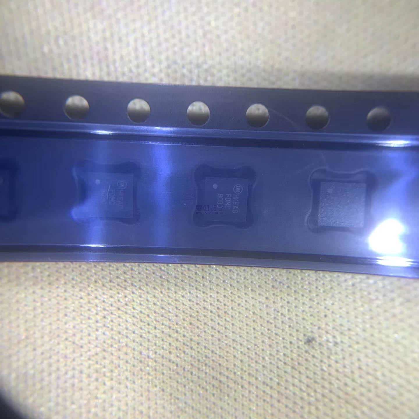




FDMC8030


N-channel MOSFET, 30V 11A, RDS(on) 11mΩ@10V, PowerTrench, DFN-8 3.3x3.3mm, onsemi FDMC8030

5400

Effective Inventory
Go to Inquiry

Image for reference only

Manufacturer Part:

FDMC8030

Package:

DFN-8 (Dual Flat No-lead, 8 pins), 3.3mm × 3.3mm × 0.8mm, exposed pad, tape and reel

Brand:
Product Categories:
Other recommendations you may be interested in.
Description

Product Overview

The FDMC8030 is an N-channel enhancement mode power MOSFET from ON Semiconductor, featuring PowerTrench® technology for high performance in a compact DFN-8 package. This device is rated for 30 V drain-source voltage and 11 A continuous drain current (at 25°C), with extremely low on-resistance RDS(on) of 11 mΩ maximum at VGS = 10 V and 14 mΩ maximum at VGS = 4.5 V. The PowerTrench MOSFET technology delivers fast switching speed, low gate charge (11 nC typical), low output capacitance, and high power density — optimizing efficiency in high-frequency switching applications. Housed in an 8-pin DFN package (3.3mm × 3.3mm), the FDMC8030 offers excellent thermal performance in a small footprint, making it ideal for DC-DC converters, load switches, motor drives, battery management systems, power management, and other high-efficiency power applications.

Key Specifications

Parameter Value
Manufacturer ON Semiconductor (onsemi)
Part Number FDMC8030
Product Type N-Channel Enhancement Mode Power MOSFET
Technology PowerTrench® MOSFET
Drain-Source Voltage (VDS) 30 V
Gate-Source Voltage (VGS) ±20 V
Continuous Drain Current (ID) 11 A @ 25°C; 8.5 A @ 100°C
Pulsed Drain Current (IDM) 44 A
Drain-Source On-Resistance (RDS(on)) 11 mΩ max @ VGS = 10V, ID = 11A
RDS(on) @ 4.5V 14 mΩ max @ VGS = 4.5V, ID = 8.5A
Gate Threshold Voltage (VGS(th)) 1.5 V typical (0.9V~2.0V range)
Total Gate Charge (Qg) 11 nC typical @ VGS = 10V
Gate-Drain Charge (Qgd) 3.5 nC typical
Gate-Source Charge (Qgs) 2.5 nC typical
Input Capacitance (Ciss) 850 pF typical @ VDS = 15V, VGS = 0V
Output Capacitance (Coss) 230 pF typical
Reverse Transfer Capacitance (Crss) 95 pF typical
Body Diode Forward Voltage 0.85 V typical @ IS = 11A
Diode Reverse Recovery Time (trr) Fast body diode
Total Power Dissipation (PD) 2.5 W @ 25°C (DFN-8 package)
Thermal Resistance (Junction to Ambient) RθJA ≈ 50°C/W (on standard PCB)
Thermal Resistance (Junction to Pad) RθJC ≈ 4°C/W
Maximum Junction Temperature +175°C
Operating Temperature Range -55°C ~ +175°C
Package / Case Style DFN-8 (Dual Flat No-lead, 8 pins)
Package Dimensions 3.3 mm × 3.3 mm × 0.8 mm (approximate)
Mounting Type Surface Mount (SMD / SMT)
RoHS RoHS Compliant / Lead-free
Halogen Free Yes
Packaging Tape and reel
Product Status Active

Features

  • N-channel enhancement mode power MOSFET
  • PowerTrench® technology for high performance
  • 30 V drain-source voltage rating
  • 11 A continuous drain current @ 25°C
  • Ultra-low on-resistance: 11 mΩ @ VGS=10V
  • 4.5 V gate drive capability (14 mΩ @ 4.5V)
  • Low gate charge: 11 nC typical
  • Fast switching speed
  • High power density in compact package
  • Fast body diode with low recovery
  • 850 pF input capacitance
  • 230 pF output capacitance
  • Exposed DFN pad for excellent thermal
  • 3.3mm × 3.3mm DFN-8 package
  • 2.5 W power dissipation @ 25°C
  • High 175°C junction temperature rating
  • RoHS compliant / lead-free
  • Halogen free
  • Tape and reel packaging
  • Ideal for high-efficiency DC-DC converters

Applications

  • DC-DC converters (buck, boost, synchronous rectifiers)
  • Load switches and power distribution
  • Battery management systems (BMS)
  • Motor drives and motor control
  • Power management IC (PMIC) companion
  • Portable electronics and computing
  • LED drivers and lighting
  • Server and telecom power systems
  • Switch mode power supplies (SMPS)
  • High-efficiency power switching

The FDMC8030 is an N-channel enhancement mode power MOSFET from ON Semiconductor’s PowerTrench® family, designed for high-efficiency power switching applications in consumer, computing, and industrial electronics. PowerTrench technology is ON Semi’s advanced trench MOSFET architecture that delivers an optimized combination of low on-resistance (RDS(on)), low gate charge (Qg), low output capacitance (Coss), and fast switching speed — all critical parameters for achieving high efficiency in high-frequency power conversion. The FDMC8030 is rated for 30 V drain-source voltage and 11 A continuous drain current at 25°C, derated to 8.5 A at 100°C junction temperature. Its low on-resistance of 11 mΩ maximum at 10 V gate drive and 14 mΩ maximum at 4.5 V gate drive enables low conduction losses, while the low gate charge of 11 nC typical minimizes switching losses — an important balance for overall efficiency in DC-DC converter applications. The 4.5 V gate drive capability makes the device suitable for both 5 V and 12 V gate drive systems commonly found in computing and telecom power applications. The DFN-8 package (3.3 mm × 3.3 mm) provides an excellent combination of compact size and thermal performance. The exposed bottom pad of the DFN package provides a low thermal resistance path from the die to the PCB, enabling effective heat dissipation and allowing the device to handle its rated power in a small footprint. With 8 pins (multiple source and drain connections), the package also provides multiple parallel current paths for lower package resistance and improved current distribution. Key features include a fast body diode with low reverse recovery charge, which is important for synchronous rectifier and half-bridge applications where the body diode conducts during dead time. The device is fully characterized for both static and dynamic parameters including capacitances, gate charge characteristics, switching times, and safe operating area (SOA). With an operating temperature range of -55°C to +175°C and a high junction temperature rating of 175°C, the FDMC8030 provides substantial thermal headroom for demanding applications. RoHS compliant, lead-free, and halogen-free, it is packaged in tape and reel for high-volume automated assembly. Overall, the FDMC8030 is a versatile 30V N-channel MOSFET that finds application in DC-DC converters, load switches, battery management, motor drives, and power management circuits where high efficiency and small size are required.

The FDMC8030 is an N-channel enhancement mode MOSFET (Metal-Oxide-Semiconductor Field-Effect Transistor) that operates as a voltage-controlled switch. In an N-channel MOSFET, current flows between the drain and source terminals through a channel of N-type semiconductor material, and the conductivity of this channel is controlled by the voltage applied to the gate terminal. The gate is electrically insulated from the channel by a thin layer of silicon dioxide (the ‘oxide’ in MOSFET), so the gate draws essentially zero DC current — only a small charging current when switching. In enhancement mode, the channel is normally non-conducting (off) when the gate-source voltage (VGS) is 0 V. When a positive VGS is applied that exceeds the gate threshold voltage (VGS(th), typically 1.5 V for FDMC8030), an electric field forms between the gate and the semiconductor, attracting electrons to the region under the gate oxide and creating a conductive N-type channel between the drain and source. The higher the VGS above threshold, the wider and more conductive the channel becomes, resulting in lower on-resistance (RDS(on)). ON Semiconductor’s PowerTrench technology uses a trench (vertical) gate structure rather than a planar (horizontal) structure. In the trench structure, the gate electrode is formed in a trench etched vertically into the silicon, with the gate oxide lining the trench walls. This vertical structure has several advantages: the channel is formed along the vertical trench walls, which increases the effective channel width per unit of die area (reducing RDS(on) for a given die size); the gate-to-drain overlap capacitance (Crss) is reduced, improving switching speed and reducing switching losses; and the overall die can be smaller for a given RDS(on) rating, reducing cost. When the MOSFET is fully on (saturated, with VGS well above threshold), it behaves like a low-value resistor (RDS(on)), and power dissipation is I² × RDS(on). This is the conduction loss. When switching between on and off states, energy is dissipated as the voltage and current transition — these are the switching losses, which depend on gate charge, output capacitance, and switching frequency. The FDMC8030’s low gate charge and low output capacitance minimize these switching losses, which is particularly important in high-frequency DC-DC converter applications. The body diode (also called the parasitic diode or intrinsic diode) is formed by the body-drain PN junction inherent in the MOSFET structure. It conducts when the drain-source voltage goes negative (for an N-channel device), and its characteristics are important in synchronous rectifier and bridge applications where the body diode carries current during dead time. The fast body diode of the FDMC8030 reduces losses in these applications. Overall, the PowerTrench architecture provides an optimal balance of low conduction loss, low switching loss, and high power density.

The FDMC8030 is an N-channel power MOSFET in an 8-pin DFN (Dual Flat No-lead) surface-mount package with exposed thermal pad.

Pin Designation Description
Pins 1-4 Gate (G) + NC Pin 4 is Gate; Pins 1-3 are typically No Connect or source in DFN-8
Pins 5-8 Drain (D) Multiple drain pins connected together for high current
Exposed Pad Source (S) Large exposed pad on bottom = Source connection (also for thermal)

Note: In typical DFN-8 power MOSFET pinouts, one side contains the gate pin(s), the opposite side contains multiple drain pins, and the large exposed bottom pad serves as both the source connection and the primary thermal path. Exact pin assignments should be verified against the official datasheet.

Package Features:

  • Package Style: DFN-8 (Dual Flat No-lead, 8 connections)
  • Package Dimensions: 3.3 mm × 3.3 mm × 0.8 mm (approximate)
  • Exposed Thermal Pad: Yes (large bottom pad for heat dissipation)
  • Termination: Tin-plated, lead-free
  • Mounting: Surface mount technology (SMT)
  • Thermal Resistance (Junction to Case): ~4°C/W (excellent thermal performance)
  • Current Handling: Multiple drain and source connections for low resistance
  • Packaging: Tape and reel (standard for SMT assembly)
  • Weight: Lightweight
  • RoHS Compliant: Yes
  • Halogen Free: Yes

Application Notes:

  • Use wide copper traces on drain and source for low resistance and good heat spreading
  • Maximize copper area on the source pad for thermal dissipation
  • Place gate resistor close to the gate pin for damping and noise immunity
  • Ensure adequate PCB thermal vias under the exposed pad
  • Refer to the ON Semiconductor FDMC8030 datasheet for exact pinout, dimensions, recommended PCB footprint, and thermal design guidelines
  • DC-DC Converters: Used as the control switch or synchronous rectifier in buck, boost, buck-boost, and other DC-DC converter topologies in computing, telecom, and consumer electronics, where the low RDS(on) and low gate charge combine for high efficiency across light and heavy load conditions
  • Load Switches & Power Distribution: Deployed as high-side or low-side load switches in portable electronics, servers, and communication equipment for power distribution, enabling and disabling power rails to subsystems, and providing protection features like current limiting and voltage monitoring
  • Battery Management Systems (BMS): Used in battery management systems for Li-ion battery packs (laptops, power tools, e-bikes, EV modules) as discharge/control FETs, cell balancing switches, and protection circuit switches, leveraging the 30V rating for multi-cell battery stacks
  • Motor Drives & Motor Control: Found in BLDC and brushed DC motor drive circuits for power tools, robotics, drones, and automotive actuators, where high current capability and efficient switching contribute to extended battery life and high performance
  • Power Management IC Companions: Used alongside power management ICs (PMICs) as external pass transistors for high-current power rails, or as additional switching regulators controlled by the PMIC’s PWM outputs
  • Portable Electronics & Computing: Used in laptops, tablets, smartphones (high-power variants), wearables, and accessories for efficient power conversion, battery charging, and power management in space-constrained designs where the small DFN-8 package is essential
  • LED Drivers & Lighting: Deployed in LED driver circuits for general lighting, automotive lighting, and display backlighting as the switching element in buck, boost, and buck-boost LED driver topologies, providing efficient constant-current drive for LED arrays
  • Server & Telecom Power: Used in server power supplies, telecom rectifiers, and datacom equipment for intermediate bus converters, point-of-load regulators, and power OR-ing applications where efficiency and power density are critical design requirements
Part Number Manufacturer VDS ID @25°C RDS(on) max Package
FDMC8030 ON Semi 30V 11A 11mΩ @ 10V DFN-8 (3.3×3.3)
FDMC8420 ON Semi 30V 17A 7.6mΩ @ 10V DFN-8 (3.3×3.3)
FDV301N ON Semi 25V 2.5A 80mΩ @ 4.5V SOT-23
SI7134DP Vishay 30V 12A 10.5mΩ @ 10V PowerPAK SO-8
AO3400A Alpha & Omega 30V 5.8A 25mΩ @ 10V SOT-23-3L
IRLML6246TRPBF Infineon 20V 16A 7.2mΩ @ 4.5V TSOP-6
Recommend Parts
Three-phase bridge rectifier, 50A, 1600V, MT-35A QC terminal package, industrial power supply

Brand:

Package:

MT-35A (4-Square QC terminal, ~35x60mm base)

In stock:

5600pcs

Cargo cycle: 3~7 Days
The minimum order is 1

Go to Inquiry
PNP high-voltage audio transistor, 350V VCEO, 15A IC, 230W, 30MHz fT, TO-264, audiophile grade

Brand:

Package:

TO-264 / TO-3P (15.75 x 20.0 mm, 4.83mm height)

In stock:

5100pcs

Cargo cycle: 3~7 Days
The minimum order is 1

Go to Inquiry
NPN high-voltage audio transistor, 350V VCEO, 15A IC, 230W, 30MHz fT, TO-264, audiophile grade

Brand:

Package:

TO-264 / TO-3P (15.75 x 20.0 mm, 4.83mm height)

In stock:

5200pcs

Cargo cycle: 3~7 Days
The minimum order is 1

Go to Inquiry
NPN power transistor, 250V VCEO, 16A IC, 200W, perforated emitter, low THD, TO-264 package

Brand:

Package:

TO-264 / TO-3P (15.75 x 20.0 mm, 4.83mm height)

In stock:

6800pcs

Cargo cycle: 3~7 Days
The minimum order is 1

Go to Inquiry
PNP power transistor, 250V VCEO, 16A IC, 200W, perforated emitter, low THD, TO-264 package

Brand:

Package:

TO-264 / TO-3P (15.75 x 20.0 mm, 4.83mm height)

In stock:

6500pcs

Cargo cycle: 3~7 Days
The minimum order is 1

Go to Inquiry
NPN Darlington transistor, 300V VCEO, 1.5A IC, hFE=15000 typical, DPAK surface mount package

Brand:

Package:

DPAK / TO-252-3 (6.5 x 6.22 mm, 2.45mm height)

In stock:

11800pcs

Cargo cycle: 3~7 Days
The minimum order is 1

Go to Inquiry
Quality Assurance

Quality is the core foundation of our long-term global cooperation. With over 20 years of experience in the electronic component industry, Materialparts has built a strict and standardized quality management system covering component sourcing, incoming inspection, full-batch testing, packaging and delivery. We are committed to delivering 100% genuine, high-reliability electronic components for industrial control, automotive electronics, consumer electronics and medical device industries, and fully safeguarding your production and R&D projects.

1. Authorized & Genuine Sourcing Promise

All of our electronic components are procured from official authorized distributors and original manufacturers. We strictly reject counterfeits, refurbished parts, disassembled components and gray-market goods. Every product is guaranteed to be brand-new original parts and fully consistent with the original technical parameters. For branded products such as NXP IC series, we maintain complete supply channel documents to realize full product traceability.

2. Strict Full-batch Quality Inspection

We implement 100% full-batch quality control for all goods before shipment. Our professional QC team conducts multi-dimensional tests including appearance inspection, electrical parameter testing, performance verification and packaging check. Each batch of components is attached with complete inspection reports and batch records. We stick to zero-tolerance standards for defective products to ensure every piece of component meets industrial application requirements.

3. Industry Standard Compliance

Our products comply with a variety of international industry quality standards to adapt to high-standard application scenarios:
  • Automotive Electronics: All automotive-grade components pass AEC-Q series certification, featuring excellent stability and durability to adapt to complex vehicle operating environments.
  • Medical Devices: High-reliability components meet medical industry safety and compliance regulations, ensuring stable operation for medical equipment.
  • Industrial Control & Consumer Electronics: Products conform to universal international electronic industry standards, suitable for long-term continuous operation of various equipment.

4. Professional Reliability Control

For static-sensitive, moisture-sensitive and precision components such as ICs, PCBs, sensors and connectors, we carry out reliability screening in advance. Combined with standardized ESD anti-static packaging and vacuum moisture-proof packaging, we avoid component damage caused by static electricity, dampness or collision during storage and transportation, and retain the original performance of products.

5. Traceability Management System

We establish a complete product traceability system. Each batch of goods corresponds to independent batch number, sourcing record, inspection record and delivery record. Customers can query the whole lifecycle information of components at any time. This system effectively solves quality risks and facilitates after-sales handling and production quality control for your company.

6. After-sales Quality Guarantee

If any product is confirmed to have non-conformity quality problems due to our reasons after receipt, we provide free return, exchange and supplementary delivery services. Our professional quality team will also conduct root cause analysis to optimize our quality control process. We respond to quality feedback within 24 hours to resolve your worries efficiently.

Contact Us

If you have inquiries about our quality standards, inspection procedures or product certification documents, please feel free to contact us:


Email: info@ic-vendor.com
Tel / WhatsApp: +86 13760382860
Address: Room 2919, Guoli Building, Huaqiang North, Futian District, Shenzhen, Guangdong, China


Shipping & Payment

Materialparts is a professional global supplier of electronic components with over 20 years of industry experience. We provide one-stop supply of passive components, integrated circuits, as well as parts for industrial control, automotive electronics, consumer electronics and medical devices. Below are the unified shipping and payment policies applicable to all orders, samples and bulk purchases worldwide.

1. Payment Terms

We offer a variety of secure and convenient payment methods to meet diverse business cooperation needs. Details are as follows:
  1. Accepted Payment Methods
  • T/T (Bank Wire Transfer): The primary settlement method for bulk orders and a widely used international payment channel.
  • PayPal: Ideal for small orders, sample orders and quick payments.
  1. Settlement Currency


    US Dollar (USD) is the default settlement currency. RMB is available for domestic customers.

  2. Bank Charges


    All transfer fees, intermediary bank charges and other remittance-related expenses shall be borne by the buyer.

  3. Payment Requirements
  • Sample and small orders: Shipment will be arranged upon full payment.
  • In-stock bulk orders: Goods will be delivered within 2 to 3 working days after full payment.

2. Shipping & Delivery

We partner with leading global logistics providers to ensure safe and fast delivery worldwide. Relevant details are listed below:
  1. Logistics Partners
  • International Express: DHL, FedEx, UPS, TNT
  • Economy Logistics: Air freight and sea freight for large-volume cargo
  • Domestic Delivery: SF Express, Yunda Express
  1. Order Processing Time
  • In-stock items: Orders confirmed and fully paid before 14:00 (GMT+8) will be shipped on the same day. All other orders will be dispatched within 1 to 2 working days.
  • Out-of-stock or sourced items: The delivery lead time will be confirmed separately according to brand and inventory status.
  1. Estimated Transit Time
  • International Express: 3 – 7 working days globally
  • Air Freight: 7 – 12 working days
  • Sea Freight: 25 – 40 working days for heavy and large bulk cargo
  1. Shipping Fee Rules
  • Shipping cost is calculated based on package weight, volume, destination and delivery method.
  • Both freight prepaid and freight collect are available. Please provide your courier account number in advance if you choose freight collect.
  • Free international express delivery is offered for large orders. Terms for long-term partners can be negotiated separately.
  1. Shipment Tracking
     

    Within 24 hours after dispatch, we will send the tracking number, commercial invoice, packing list and other documents to your email or communication account. You may check the shipment status online in real time.

3. General Order Rules & Notes

  1. MOQ & Sample Service


    We support flexible minimum order quantities for samples, small-batch and large-batch orders. All sample orders shall comply with the above shipping and payment policies.

  2. Packaging Standard


    All electronic components are packed with professional anti-static and shockproof materials. Original factory packaging is available for branded chips and integrated circuits.

4. Customs & Liability Statement

  1. Import Duties & Taxes


    All import duties, customs clearance fees and local taxes incurred for international shipments shall be borne by the buyer. We will provide complete customs documents to assist you with clearance procedures.

  2. Handling of Lost or Damaged Goods
  • In case of loss or severe damage during transit, please contact us within 48 hours after receiving the tracking information. We will assist you in filing a claim with the logistics provider.
  • We shall not be liable for any losses caused by incorrect delivery address, wrong contact information or the buyer’s refusal to complete customs clearance.

5. Local Pickup in Shenzhen

Local pickup service is available for customers in Shenzhen and surrounding areas:
  • Address: Room 2919, Guoli Building, Huaqiang North, Futian District, Shenzhen, Guangdong Province, China
  • Business Hours: 09:00 – 18:00, Monday to Friday. Closed on weekends and official public holidays.
  • Notice: Please make an appointment via email or communication tools one day in advance, and present your order information upon pickup.

Contact Information

Email: info@ic-vendor.com

Tel / WhatsApp: +86 13760382860

Service & Packaging

Materialparts is a professional electronic component supplier based in Shenzhen, China, with over 20 years of global trading experience. We integrate component procurement, quality inspection, technical support, customized packaging, and global delivery services to provide one-stop supply chain solutions. Our business covers industrial control, automotive electronics, consumer electronics, medical devices and other industries. We always adhere to genuine sources, stable supply and considerate after-sales service.

Core Services

1. One-stop Sourcing & BOM Support

We specialize in a full range of passive and active electronic components, including SMD resistors, power resistors, connectors, aviation connectors, LED beads, flexible circuit boards, printed circuit boards, and integrated circuits. Our professional team provides BOM list consolidation, component matching, and alternative model recommendation services. We support sample orders, small-batch trial production, and mass production orders with flexible MOQs to meet diverse procurement needs.

2. Genuine Product Guarantee & Full-process Quality Inspection

All products are sourced from official authorized channels and are 100% original genuine parts. Every batch of goods undergoes strict full-process quality inspection before delivery, with complete batch records and traceability documents provided. Our products comply with AEC-Q standards for automotive electronics and high-reliability specifications for medical devices. We eliminate counterfeits, refurbished parts and defective products from the source to secure your project production.

3. Fast Quotation & Order Processing

Our customer service team responds promptly to inquiries and quotation requests. All in-stock orders will be processed within one working day. We provide stocking reservation services for long-term cooperative customers, effectively solving problems such as component shortages and unstable supply chains.

4. Professional Technical Support

Our senior engineer team provides free technical consultation, model selection guidance and original manufacturer datasheets. We assist customers in solving problems related to product R&D, circuit design and component application, providing reliable technical support for project progress.

5. Sourcing for Special Components

Relying on our global supply chain network, we professionally source scarce components, obsolete parts and customized special components to efficiently solve your procurement difficulties.

6. Global Logistics & Document Services

We cooperate with mainstream international logistics providers including DHL, FedEx, UPS and TNT to achieve fast global delivery. We can provide complete export documents such as customs declaration files, commercial invoices and packing lists to ensure smooth customs clearance for international shipments. Local pickup is also available for customers in Shenzhen, China.

Professional Packaging Standards

Electronic components are sensitive to static electricity, collision, moisture and dust. We adopt industry-standard anti-static packaging solutions to fully ensure the integrity of goods during transportation and storage.

1. General Packaging Specifications

  • All components are packed separately to avoid damage caused by friction and collision;
  • Shockproof buffer materials are added for fragile products to ensure transportation safety;
  • Each package is clearly marked with part number, quantity, batch number and specifications for easy inventory counting and management.

2. Classified Professional Packaging

  • Anti-static Packaging: Static-sensitive components such as chips, circuit boards and sensors are packaged with anti-static bags, shielding boxes and conductive foam in strict accordance with international anti-static standards to prevent static damage.
  • Vacuum Moisture-proof Packaging: Moisture-sensitive components are vacuum-sealed with desiccants to isolate humid air, suitable for ocean transportation and long-term storage.
  • Original Factory Packaging: Integrated circuits of brands such as NXP are delivered with original reels, trays or tubes by default, retaining complete original packaging and adapting to automated SMT production lines.
  • Discrete Device Packaging: Discrete devices such as SMD resistors, power resistors and LEDs are quantitatively and classifiedly packaged with accurate quantity and clear marking.
  • Connector / Aviation Connector Packaging: Hard outer packaging is adopted to prevent pin bending and structural deformation.

3. Custom Packaging Services

We provide value-added services including personalized packaging, custom labeling and re-reeling according to customer requirements, fully matching your production and warehouse management standards.

Contact Information

For service consultation or packaging customization, please feel free to contact us:
Email: info@ic-vendor.com
Tel / WhatsApp: +86 13760382860
Address: Room 2919, Guoli Building, Huaqiang North, Futian District, Shenzhen, Guangdong, China
 

Online Inquiry Form

Support Excel, PDF, CSV format files for full BOM list quotation

Submit your component procurement and custom packaging needs via the form below. We will provide a detailed quotation and professional solution within 1–8 working hours.