


Product Overview
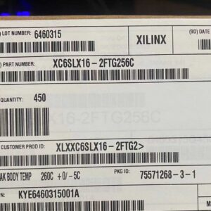
The XC6SLX16-2FTG256C-1 is a Spartan-6 LX FPGA from Xilinx (AMD), featuring 14,579 logic cells in a 256-pin Fine-Pitch Thin BGA (FTBGA) package. As a member of the cost-optimized Spartan-6 family built on 45 nm low-power copper process technology, this device delivers an excellent balance of logic capacity, DSP performance, memory resources, and I/O count for high-volume, cost-sensitive applications.
The XC6SLX16 architecture includes 2,278 CLB slices with 18,224 flip-flops, 32 DSP48A1 slices for digital signal processing (each with an 18×18 multiplier, adder, and accumulator), and 32 block RAMs totaling 576 Kb of embedded memory. Two Clock Management Tiles (CMTs) provide flexible clock generation with DCMs and PLLs, while two integrated memory controller blocks support DDR/DDR2/DDR3/LPDDR interfaces at up to 800 Mb/s data rate.
The FTG256 package is a compact 17 x 17 mm fine-pitch BGA with 1.0 mm ball pitch, providing up to 200 user I/O pins across 4 I/O banks. The device supports over 40 I/O standards including LVCMOS, LVTTL, HSTL, SSTL, and LVDS differential signaling. The -2 speed grade is rated for commercial temperature range (0 degC to 85 degC). AMD has committed to long-term Spartan-6 supply through at least 2030, making it suitable for long-lifecycle industrial and automotive programs.
Key Specifications
| Parameter | Value |
|---|---|
| Logic Cells | 14,579 |
| CLB Slices | 2,278 (569 SLICEM + 1,709 SLICEL) |
| Flip-Flops | 18,224 |
| Distributed RAM (max) | 136 Kb |
| Block RAM (18 Kb blocks) | 32 blocks = 576 Kb total |
| DSP48A1 Slices | 32 (18×18 multiplier + accumulator) |
| Clock Management Tiles | 2 (each: 2 DCM + 1 PLL) |
| Memory Controller Blocks | 2 (DDR/DDR2/DDR3/LPDDR, 800 Mb/s) |
| GTP Serial Transceivers | 0 (LX family, no serial transceivers) |
| I/O Banks | 4 banks |
| Max User I/Os (FTG256) | 200 single-ended / 86+ differential pairs |
| Max LVDS Data Rate | 1,080 Mb/s per pair |
| Core Supply Voltage (VCCINT) | 1.2 V (1.14 V to 1.26 V) |
| Auxiliary Supply (VCCAUX) | 2.5 V |
| I/O Supply (Vcco) | 1.2 V to 3.3 V (bank-independent) |
| Speed Grade | -2 (second fastest commercial grade) |
| Configuration Methods | SPI x1/x2/x4, BPI up to x16, JTAG, Master Serial |
| Package | FTG256 / FTBGA-256 (17×17 mm, 1.0 mm pitch) |
| Operating Temperature | 0 degC to +85 degC (commercial, C suffix) |
Features
- Spartan-6 LX FPGA: cost-optimized logic density
- 14,579 logic cells with dual-register 6-input LUTs
- 32 DSP48A1 slices for high-performance DSP
- 576 Kb block RAM + 136 Kb distributed RAM
- 2 CMTs (2 DCMs + 1 PLL each) for flexible clocking
- 2 integrated DDR/DDR2/DDR3 memory controllers
- Up to 200 user I/O pins in FTG256 package
- 40+ I/O standards: LVCMOS, LVTTL, HSTL, SSTL, LVDS
- Adjustable I/O slew rate and drive strength (up to 24 mA)
- Hot-swap compliant I/O banks
- Device DNA unique identifier for anti-cloning
- MultiBoot support with watchdog protection
- AES bitstream encryption (larger devices)
- Multiple power-saving modes: Suspend, Hibernate
- MicroBlaze 32-bit soft processor support
- 45 nm low-power copper process
- ISE Design Suite compatible
- Long-term availability: through 2030+
- FTBGA-256 package, lead-free, RoHS compliant
Applications
- Industrial automation and PLC systems
- Automotive infotainment and driver information
- Video and display processing
- Cost-effective interface bridging
- Consumer electronics and DTV/STB
- Motor control and motion controllers
- Data acquisition and instrumentation
- Medical electronics and imaging