


Product Overview
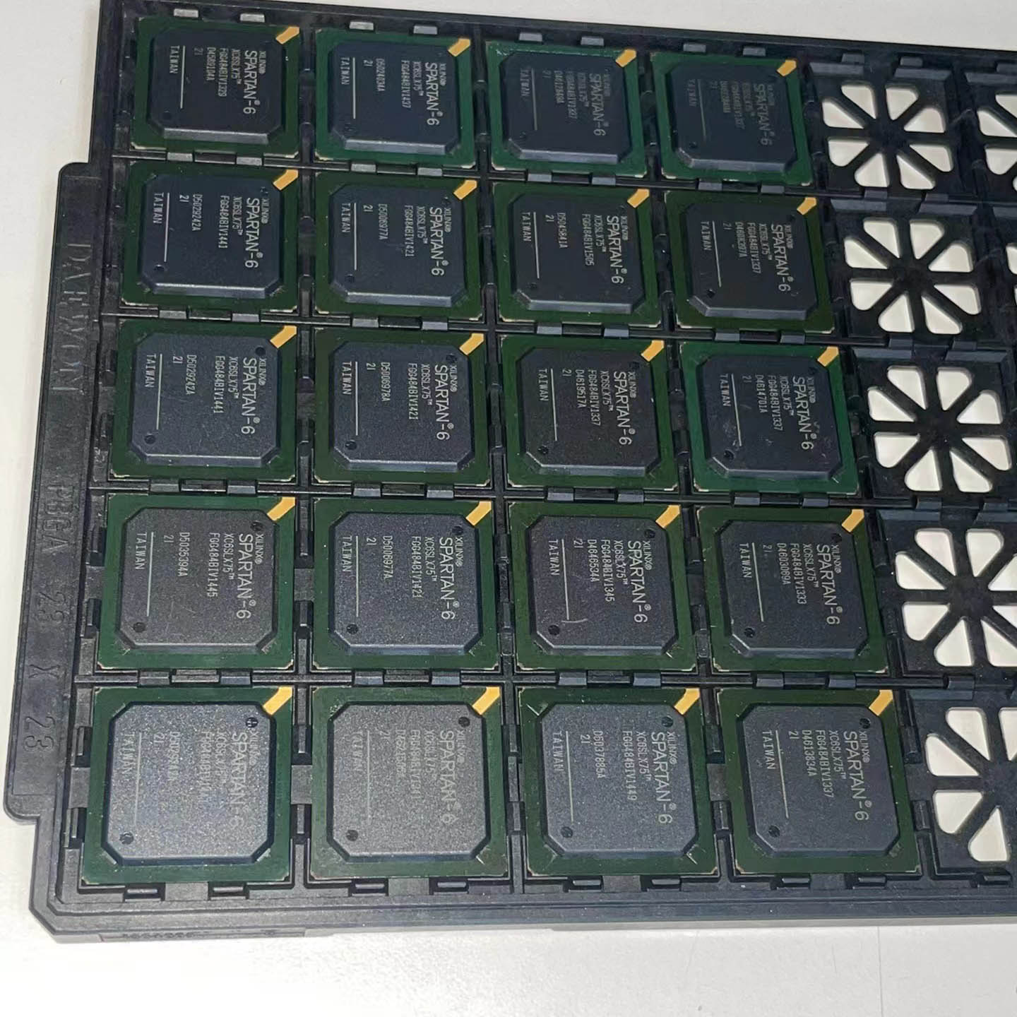
The XC6SLX75-2FGG484I is a high-density Spartan-6 LX FPGA from Xilinx (AMD), featuring 74,637 logic cells in a 484-ball Fine-pitch BGA (FGG484) package. As one of the largest devices in the Spartan-6 LX family, it delivers substantial logic resources, DSP processing power, and memory capacity while maintaining the cost-optimized positioning of the Spartan-6 platform.
Built on 45 nm low-power copper process technology, the XC6SLX75 integrates 11,648 CLB slices with 93,184 flip-flops, 132 DSP48A1 slices for high-performance digital signal processing, and 172 block RAMs totaling 3,096 Kb of embedded memory. Four Clock Management Tiles (CMTs) provide comprehensive clock synthesis with DCMs and PLLs, while two integrated memory controller blocks support DDR/DDR2/DDR3/LPDDR interfaces at up to 800 Mb/s data rate.
The FGG484 package measures 23 x 23 mm with 1.0 mm ball pitch, providing up to 408 user I/O pins across 6 I/O banks, supporting over 40 I/O standards including LVCMOS, LVTTL, HSTL, SSTL, and LVDS differential signaling. The -2 speed grade with industrial temperature range (-40 degC to +100 degC junction) makes this device suitable for demanding industrial, automotive, and communications applications. AMD guarantees Spartan-6 long-term availability through at least 2030.
Key Specifications
| Parameter | Value |
|---|---|
| Logic Cells | 74,637 |
| CLB Slices | 11,648 (2,908 SLICEM + 8,740 SLICEL) |
| Flip-Flops | 93,184 |
| Distributed RAM (max) | 696 Kb |
| Block RAM (18 Kb each) | 172 blocks = 3,096 Kb total |
| DSP48A1 Slices | 132 (18×18 multiplier + adder + accumulator) |
| Clock Management Tiles (CMT) | 4 (each: 2 DCMs + 1 PLL) |
| Memory Controller Blocks | 2 (DDR/DDR2/DDR3/LPDDR, 800 Mb/s) |
| PCIe Endpoint Block | 0 (LX variant, LXT has PCIe) |
| I/O Banks | 6 banks |
| Max User I/Os (FGG484) | 408 single-ended |
| Max LVDS Differential Pairs | 148+ pairs |
| Max I/O Data Rate | 1,080 Mb/s per LVDS pair |
| Core Voltage | 1.2 V (1.14 V to 1.26 V) |
| Auxiliary Supply | 2.5 V |
| I/O Supply Range | 1.2 V to 3.3 V (per bank) |
| Speed Grade | -2 (industrial grade) |
| Max Operating Frequency | 375 MHz |
| Configuration | SPI x1/x2/x4, BPI x16, JTAG, MultiBoot |
| Package | FGG484 / FBGA-484 (23×23 mm, 1.0 mm pitch) |
| Junction Temperature | -40 degC to +100 degC (industrial I-grade) |
Features
- Spartan-6 LX FPGA: high-density cost-optimized logic
- 74,637 logic cells with dual-register 6-input LUT architecture
- 132 DSP48A1 slices for high-performance signal processing
- 3,096 Kb block RAM + 696 Kb distributed RAM
- 4 CMTs (8 DCMs + 4 PLLs) for flexible clock management
- 2 integrated memory controllers (DDR/DDR2/DDR3/LPDDR)
- Up to 408 user I/O pins in FGG484 package (6 banks)
- 40+ I/O standards: LVCMOS, LVTTL, HSTL, SSTL, LVDS
- Up to 148+ differential LVDS pairs at 1,080 Mb/s
- Programmable I/O drive strength (up to 24 mA) and slew rate
- Hot-swap compliance on all I/O banks
- Device DNA unique identifier for design authentication
- AES bitstream encryption for design security
- MultiBoot support with watchdog for remote upgrades
- Advanced power management: Suspend, Hibernate modes
- MicroBlaze 32-bit soft processor support
- 45 nm low-power copper process technology
- ISE Design Suite design tool support
- Industrial temperature range: -40 degC to +100 degC TJ
- Long lifecycle: supported through at least 2030
- FGG484 FBGA package, lead-free, RoHS compliant
Applications
- High-end industrial automation and motion control
- Telecom and networking equipment
- Video processing and broadcast equipment
- Medical imaging and diagnostic systems
- Automotive ADAS and infotainment
- Software-defined radio and signal processing
- High-speed interface bridging and protocol conversion
- Aerospace and defense (industrial temp rated)