


Product Overview
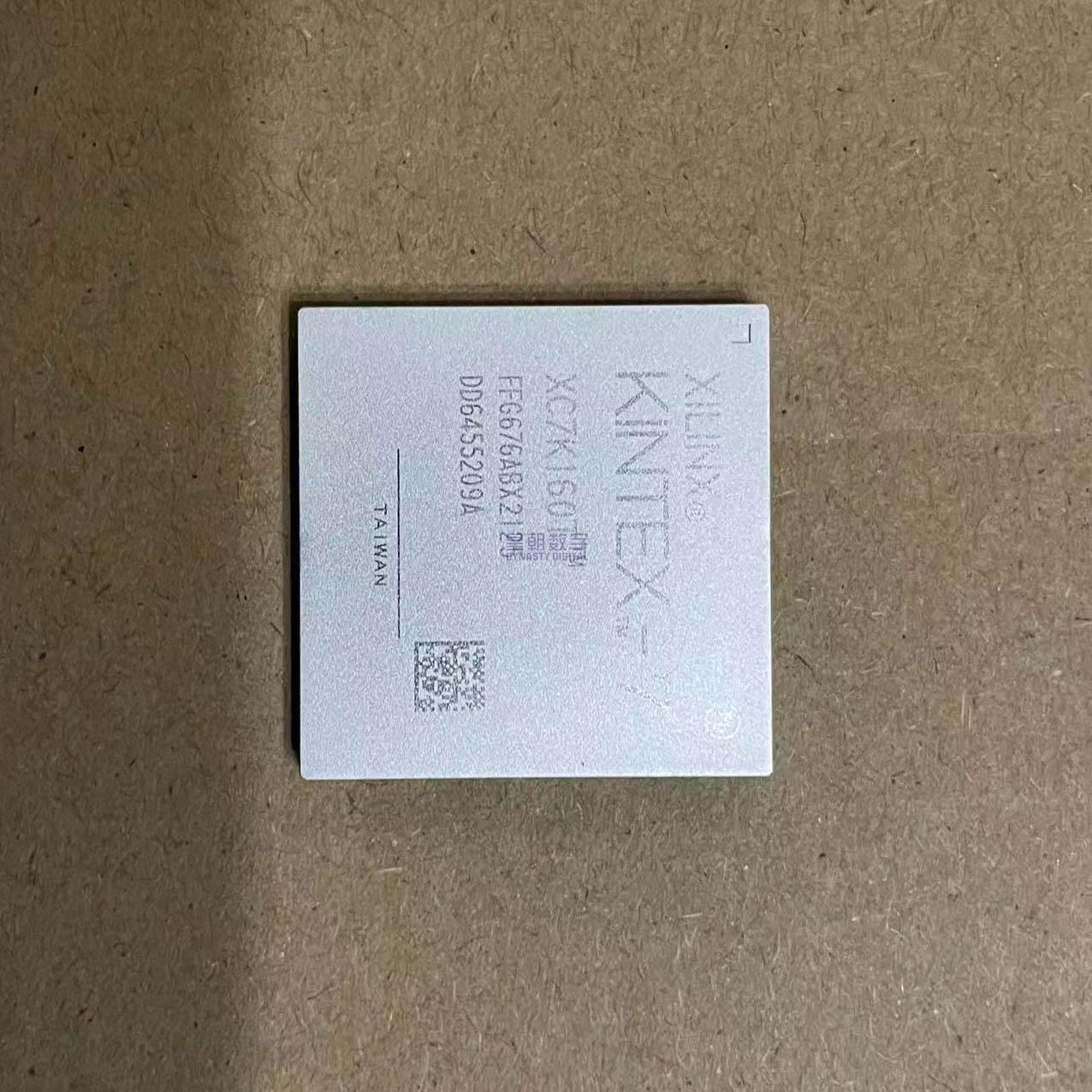
The XC7K160T-2FFG676I is a Kintex-7 FPGA from Xilinx (AMD), featuring 162,240 logic cells in a 676-ball Fine-pitch Flip-chip BGA package. As the entry-level member of the Kintex-7 family, this device delivers exceptional price-performance with high-speed serial connectivity, substantial DSP capacity, and advanced memory interfaces at a mid-range cost point.
Built on 28 nm high-k metal gate (HKMG) process technology, the XC7K160T integrates 25,350 CLB slices with 202,800 flip-flops, 600 DSP48E1 slices for high-performance signal processing, and 324 block RAMs totaling 11,664 Kb of embedded memory. Ten clock management tiles (CMTs), each containing an MMCM and a PLL, provide extensive clock synthesis capabilities. The device includes up to 16 GTX transceivers operating at up to 12.5 Gb/s (data rate dependent on speed grade), an integrated PCIe Gen2 x8 endpoint block, and a dedicated memory interface controller supporting DDR3 at up to 1,866 Mb/s.
The FFG676 package measures 27 x 27 mm with 1.0 mm flip-chip ball pitch, providing up to 500 user I/O pins across 8 high-performance (HP) banks supporting 3.3V-tolerant I/O standards. The -2 speed grade with industrial temperature range (-40 degC to +100 degC junction) delivers excellent performance for demanding communications, signal processing, and industrial applications. Kintex-7 offers the best price-performance-per-watt in the Xilinx 7-series portfolio.
Key Specifications
| Parameter | Value |
|---|---|
| Logic Cells | 162,240 |
| CLB Slices | 25,350 (202,800 flip-flops) |
| Distributed RAM (max) | ~1,980 Kb |
| Block RAM (36 Kb each) | 324 blocks = 11,664 Kb total |
| DSP48E1 Slices | 600 (25×18 multiplier + 48-bit accumulator) |
| CMT (MMCM + PLL) | 10 (10 MMCMs + 10 PLLs) |
| GTX Transceivers | 16 (up to 12.5 Gb/s each) |
| PCIe Endpoint Block | 1 (Gen2 x8, 5.0 Gb/s per lane) |
| Memory Interface Controller | 1 (DDR3/DDR3L up to 1,866 Mb/s) |
| Ethernet MACs | 2 (1G/2.5G with GMII/RGMII/SGMII) |
| I/O Banks | 8 HP banks (high-performance) |
| Max User I/Os (FFG676) | Up to 500 (3.3V tolerant HR + HP mixed) |
| Max LVDS Data Rate | 1,600 Mb/s (differential) |
| Core Voltage | 1.0 V |
| Auxiliary Voltage | 1.8 V |
| MGT AVCC | 1.0 V |
| Speed Grade | -2 (industrial I-grade) |
| Max DSP Clock | ~450 MHz (-2 speed grade) |
| Configuration | SPI x1/x2/x4/x8, BPI x16, JTAG, SelectMAP, Quad SPI |
| Package | FFG676 / FCBGA-676 (27×27 mm, 1.0 mm pitch, flip-chip) |
| Junction Temperature | -40 degC to +100 degC (industrial) |
Features
- Kintex-7 family: best price-performance-per-watt mid-range FPGA
- 162,240 logic cells with 6-input LUT architecture
- 600 DSP48E1 slices for high-performance DSP
- 11,664 Kb block RAM + ~1,980 Kb distributed RAM
- 10 CMTs with MMCMs and PLLs for comprehensive clocking
- 16 GTX transceivers: up to 12.5 Gb/s per channel
- Integrated PCI Express Gen2 x8 endpoint block
- DDR3/DDR3L memory interface: up to 1,866 Mb/s
- Dual 1G/2.5G Ethernet MACs
- Up to 500 user I/O pins across 8 banks
- 50+ I/O standards: LVCMOS, LVDS, LVPECL, HSTL, SSTL
- 1.6 Gb/s LVDS differential data rate
- AES-256 bitstream encryption, HMAC authentication
- Device DNA unique identifier for anti-cloning
- MultiBoot / Fallback configuration support
- Advanced power management: suspend / hibernate
- 28 nm HKMG process technology
- MicroBlaze 32-bit soft processor support
- Vivado Design Suite and ISE compatible
- Industrial temperature: -40 degC to +100 degC TJ
- FFG676 flip-chip BGA package, lead-free
Applications
- 4G LTE / 5G wireless infrastructure
- Wired networking and high-end routers
- Software-defined radio and radar processing
- High-end medical imaging (CT, MRI, ultrasound)
- Broadcast video infrastructure and production switching
- Aerospace and defense systems
- High-speed test and measurement equipment
- Data center FPGA acceleration