





Product Overview
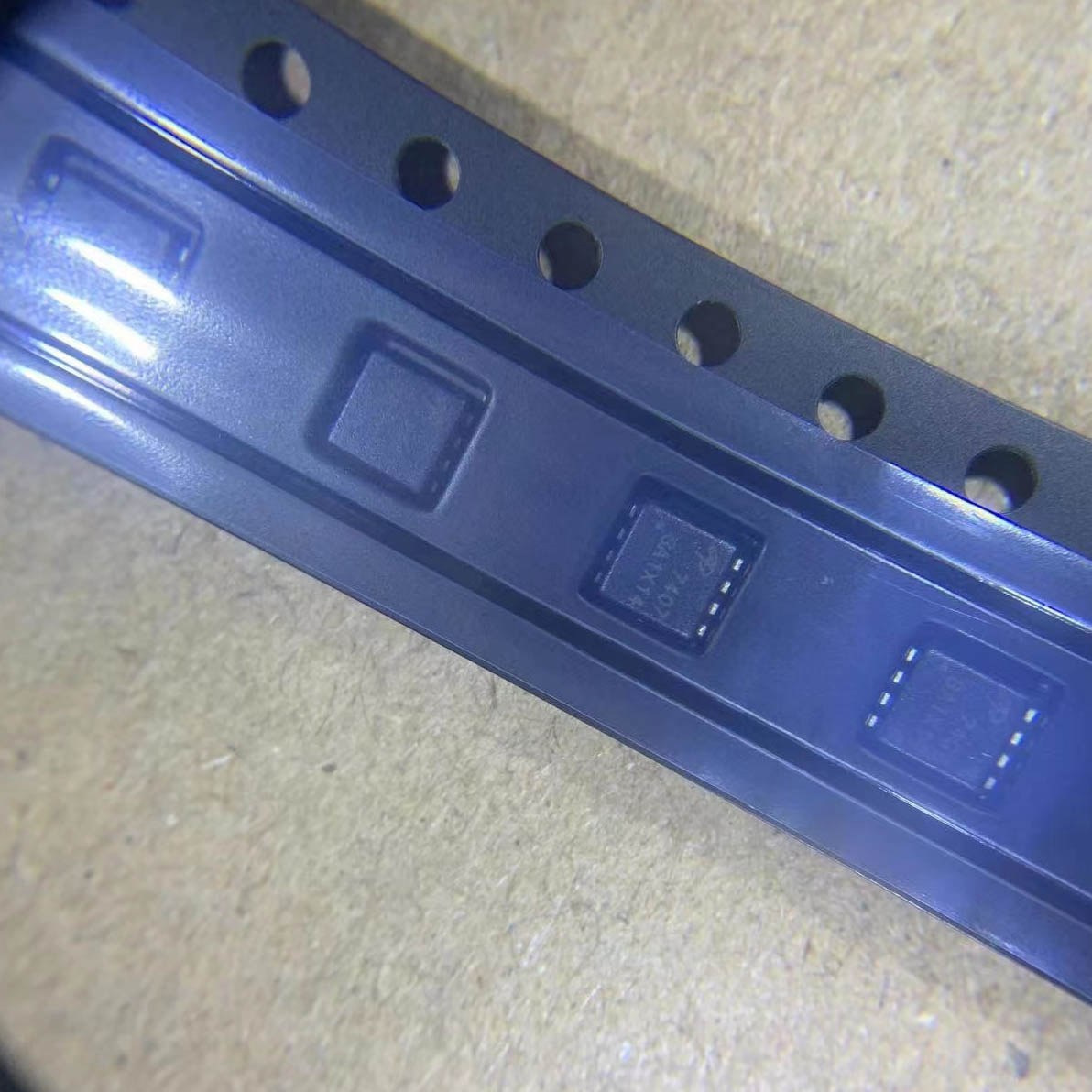
The AON7407 is a P-channel enhancement mode power MOSFET from Alpha & Omega Semiconductor, combining advanced trench MOSFET technology with a low resistance DFN package to deliver extremely low RDS(ON). The device features a 20V drain-source voltage rating and a continuous drain current of 40A at 25°C case temperature (14.5A at 25°C ambient), making it ideal for high-current load switch and battery protection applications. The AON7407 is optimized for low-voltage gate drive operation, with on-resistance specified at gate voltages as low as -1.8V, enabling efficient operation with low-voltage control signals. The device is 100% UIS (Unclamped Inductive Switching) tested and 100% Rg (Gate Resistance) tested, ensuring high reliability and consistent performance. Packaged in a compact 8-DFN-EP (3x3mm) package with exposed pad for excellent thermal performance, the AON7407 is suitable for space-constrained portable applications including tablet PCs, smartphones, notebook computers, and battery-powered devices.
Key Specifications
| Parameter | Conditions | Min | Typ | Max | Unit |
| FET Type | P-Channel Enhancement Mode | ||||
| Drain-Source Voltage (VDS) | -20 | V | |||
| Gate-Source Voltage (VGS) | ±8 | V | |||
| Continuous Drain Current (ID) | TC=25°C | -40 | A | ||
| Continuous Drain Current (ID) | TC=100°C | -29 | A | ||
| Continuous Drain Current (ID) | TA=25°C | -14.5 | A | ||
| Pulsed Drain Current (IDM) | -100 | A | |||
| Avalanche Current (IAS) | -40 | A | |||
| Power Dissipation (PD) | TC=25°C | 29 | W | ||
| Power Dissipation (PD) | TA=25°C | 3.1 | W | ||
| RDS(ON) | VGS=-4.5V, ID=-14A | 7.6 | 9.5 | mΩ | |
| RDS(ON) | VGS=-4.5V, TJ=125°C | 13.5 | mΩ | ||
| RDS(ON) | VGS=-2.5V, ID=-13A | 9.3 | 12.5 | mΩ | |
| RDS(ON) | VGS=-1.8V, ID=-11A | 11.4 | 18 | mΩ | |
| Gate Threshold Voltage (VGS(th)) | VDS=VGS, ID=-250μA | -0.3 | -0.55 | -0.9 | V |
| Zero-Gate Drain Current (IDSS) | VDS=-20V, VGS=0V | -1 | μA | ||
| Gate-Body Leakage (IGSS) | VDS=0V, VGS=±8V | ±100 | nA | ||
| Forward Transconductance (gFS) | VDS=-5V, ID=-14A | 72 | S | ||
| Diode Forward Voltage (VSD) | IS=-1A, VGS=0V | -0.52 | -1 | V | |
| Total Gate Charge (Qg) | VGS=-4.5V, VDS=-10V | 44 | 53 | nC | |
| Input Capacitance (Ciss) | VGS=0V, VDS=10V | 3495 | 4195 | pF | |
| Output Capacitance (Coss) | VGS=0V, VDS=10V | pF | |||
| Turn-On Delay (td(on)) | 18 | ns | |||
| Turn-Off Delay (td(off)) | 136 | ns | |||
| Rise Time (tr) | 32 | ns | |||
| Fall Time (tf) | 59 | ns | |||
| Junction Temperature (TJ) | -55 | 150 | °C | ||
| Package | 8-DFN-EP (3x3mm) / 8-PowerVDFN | ||||
Features
- P-channel enhancement mode MOSFET
- VDS: -20V, ID: -40A (at TC=25°C)
- Ultra-low RDS(ON): 9.5mΩ max @ VGS=-4.5V
- Excellent low-voltage drive: 12.5mΩ @ -2.5V, 18mΩ @ -1.8V
- Advanced trench MOSFET technology
- 100% UIS (Unclamped Inductive Switching) tested
- 100% Rg (Gate Resistance) tested
- High current capability: 100A pulsed drain current
- Low gate threshold voltage: -0.55V typical
- Excellent thermal performance with exposed pad
- Compact 8-DFN-EP 3x3mm package
- Green / RoHS compliant
- Halogen-free
- Optimized for load switch and battery protection
Applications
- Load switching in portable electronics
- Battery protection circuits (BMS)
- Smartphones and tablet PCs
- Notebook and ultrabook computers
- Wearable devices
- Power management and OR-ing
- DC-DC converters
- Motor control applications
- Battery-powered devices
- eReaders and portable media players